
What is a Sensor?

Digital SLR cameras capture their images on a silicon semiconductor referred to as a digital sensor. This sensor is composed of an array of photosensitive diodes called photosites that capture photons (subatomic light particles) and converts them to electrons, much like solar panels convert light to energy. This build up of electrons in each photosite is converted to a voltage which in turn is converted to digital data as a picture element or pixel. These pixels are then relayed in consecutive order and stored as an image on the cameras memory as a file. These files can then be viewed on the camera in the LCD screen, or uploaded to a computer where they can also be viewed or manipulated with imaging software.
Types of Digital Sensors
In the digital camera world there are basically two types of digital sensors: CCD and CMOS, with some new and exciting technologies on the horizon.
CCD Sensors

Charged Coupling Device (CCD) sensors were invented by Dr. Willard Boyle and Dr. George Smith at Bell Labs in 1969. Today CCD sensors are used in a multitude of devices from scanners to telescopes.
CCD sensors derive their name from how the charge is read after an image is captured. Utilizing a special manufacturing process, the sensor is able to transport the built up charge across itself without compromising the image quality. The first row of the array is read into an output register, which in turn is fed into an amplifier and an analog to digital converter. After the first row has been read, it is dumped from the read out register and the next row of the array is read into the register. The charges of each row are coupled so as each row moves down and out, the successive rows follow in turn. The digital data is then stored as a file that can be viewed and manipulated.
Until recently, CCD sensors have been predominant in digital SLRs because of their high quality/ low noise images and their maturity, having been produced for over thirty years. But new manufacturing methods of an old technology have led to inroads for it to surpass CCD sensors.
CMOS sensors
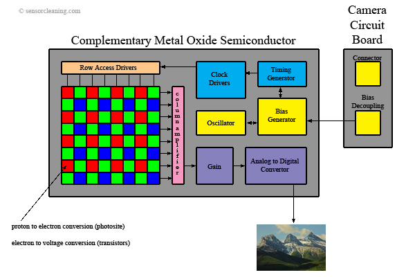
CMOS (Complimentary Metal Oxide Semiconductor) sensors or Active Pixel sensors were first discussed in length in a paper from Dr. Eric Fossum, a scientist at NASAs Jet Propulsion Laboratory, in 1992. 1993 through to 1995, JPL developed much of the technology which would be implemented into the CMOS sensor. Fossum and other members of the JPL co-founded Photobit Corporation in 1995 to commercialize the technologies they had developed. In 2001, Micron Technology acquired Photobit and used its extensive knowledge of CMOS wafer manufacturing to enhance the development further.
CMOS sensors derive their name from the way they are manufactured. They are cut from a CMOS wafer which is cheaper to produce then a CCD wafer, provides less power consumption, and also allow for more involved circuitry along side of the photosite array. Each photosite in the CMOS sensor has three or more transistors which has its benefits and its draw backs. The transistors allow for processing to be done right at the photosite, and each pixel/photosite can be accessed independently. Because the transistors occupy space on the array, some of the incoming light hits the transistors and not the photosites, which leads to picture noise. CMOS sensors also function at a very low gain which may contribute to noise.
| CCD vs. CMOS Sensors | ||
| CCD | CMOS | |
| cost | expensive to produce because of special manufacturing methods employed | inexpensive because CMOS wafers are used for many different types of semiconductors |
| power | consumes upto 100x more power than CMOS | low power consumption |
| noise | high quality, low noise images | susceptible to noise |
| maturity | produced for longer period; higher quality images, more pixels | less mature but equal in low and middle range resolutions to CCD |
| extended functionality | technically feasible; other chips are used | other circuitry easily incorporated on same chip |
| fill factor | high | low |